

Kyocera at SEMICON Europa 2026: Technologies for semiconductor manufacturing
At this year’s SEMICON Europa trade fair, which takes place in Munich, Germany, from November 10 to 13, 2026, Kyocera showcases high-precision ceramic components as well as semiconductor and optical technologies for a range of applications in the semiconductor and microelectronics industries.
- Fine Ceramic Components
- Optical Components
- Semiconductor Components
Kyoto/London − At SEMICON Europe 2026, Kyocera presents its comprehensive technology portfolio for the semiconductor and microelectronics industries. At booth # C1725 in Hall C1, the company presents its solutions for a range of requirements in semiconductor manufacturing. The focus is on high-precision ceramic components, ceramic housings and substrates, as well as optical technologies for wafer testing and chip alignment.
High-precision ceramic components for demanding process conditions
In the field of high-performance ceramics, Kyocera displays structural components, process chamber components and ceramic-metal assemblies, amongst other items. These ceramic components enable the precise realisation of complex surface profiles and structures and are characterised by high strength and low thermal expansion. They are designed to withstand a wide temperature range, rapid temperature changes and harsh process conditions. In addition to established components for the semiconductor and electronics industries, Kyocera also develops complex products to meet customer-specific requirements and, where required, provides engineering support to assist with product optimisation.

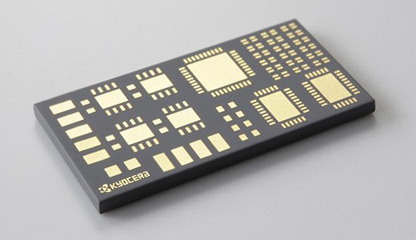
Ceramic housings and substrates for various applications
Ceramic housings and substrates for applications with high reliability requirements form another key focus of the exhibition booth. The range of applications extends from MEMS sensors – such as accelerometers, gyroscopes, inertial measurement units (IMUs), pressure and environmental sensors – to ADAS and robotics applications. Here, ceramic housings and substrates are used, amongst other things, in radar and LiDAR systems and cameras. These are complemented by heating and piezo technologies.
For SiC power modules, the portfolio includes heat sink materials and solutions with high thermal conductivity, including graphite and a water-cooled solution. Other examples include LCC packages (LCC Type Packages), multi-cavity packages (Multiple-Cavity Packages) and window lids.
Optical solutions for wafer testing and chip alignment
In the field of optics, the focus is on three inspection lenses designed for different requirements in wafer and chip inspection, as well as an optical unit for precise chip alignment.
The IR lens for inspecting 3D wafer stacks features a focus adjustment ring that allows it to be adjusted to the wafer thickness at a penetration depth of 0 to 1.2 mm. This enables the detection of internal defects and particles in the order of 1 µm. Furthermore, the design can be customised, for example with regard to the illumination. In the specification example given, the wavelength range is between 1,000 and 1,500 nm, with an objective numerical aperture (NA) of 0.5. Further specifications include a working distance of 6.23 mm, a resolution of 1.5 µm, 40× magnification, a parfocal distance of 45 mm and a field of view of 0.2208 × 0.1766 mm.
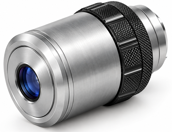
The interferometric objective is used to detect topographical defects during wafer and chip inspection. It enables high-contrast detection of defects as small as 0.1 µm and supports various interferometric methods such as Mirau and Michelson. The compact design helps to reduce the system’s footprint. Furthermore, bespoke optical designs are available for wavelength ranges from UV to near-infrared. The example specification covers a wavelength range of 420 to 540 nm, an objective-side numerical aperture (NA) of 0.5, a working distance of 3.4 mm, a resolution of less than 1 µm, a focal length of 4 mm, a parfocal distance of 45 mm and a field of view diameter of 0.5 mm.
The Plan-Apo lens, with a numerical aperture (NA) of 0.9, is designed for wafer inspection and features a high numerical aperture, a large field of view and a long working distance. The correction for chromatic aberrations reduces blurring caused by illumination, the optics are corrected to infinity. In the specification example given, the wavelength range is between 400 and 700 nm. The working distance is 1.0 mm, the magnification is 20×, the parfocal distance is 105 mm and the field of view diameter is 1.2 mm.
The three inspection lenses are supplemented by an optical unit with two fields of view for chip alignment. Two cameras and the high numerical aperture enable precise alignment to within less than 0.1 µm. The design minimises vibrations and thermal changes. The example specifications include dimensions of 186 × 156 × 40 mm (W × D × H), a working distance of 6.1 mm at both the top and bottom, 8.61× magnification, a field-of-view diameter of 1.28 mm, a numerical aperture (NA) of 0.32, a resolution of 700 line pairs per millimetre, and LED illumination. An F-THETA lens unit and aspherical lenses complete the range of optical solutions presented at the trade fair.
About SEMICON Europa 2026
SEMICON Europa is the largest and most important European trade fair for the semiconductor and microelectronics industry. It brings together the entire value chain of the sector, from materials, wafers and manufacturing equipment, through packaging technologies and chip design, to end applications. Meanwhile, the electronica 2026 trade fair will take place in Munich from 10 to 13 November 2026. KYOCERA AVX will be exhibiting there in Hall C6 at Booth # 179.
Overview – Kyocera at SEMICON Europa 2026
| Show | SEMICON Europa 2026 |
|---|---|
| Date | 10th – 13th November 2026 |
| Location | Munich, Germany |
| Kyocera's booth | Hall C1, Booth # C1725 |